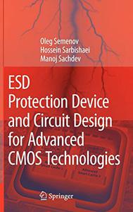
ESD Protection Device and Circuit Design for Advanced CMOS Technologies by Oleg Semenov, Hossein Sarbishaei, Manoj Sachdev
English | PDF | 2008 | 237 Pages | ISBN : 1402083009 | 9.4 MB
The challenges associated with the design and implementation of Electrostatic Discharge (ESD) protection circuits are becoming increasingly complex as technology is scaled well into nano-metric regime. Traditional approaches of ESD design may not be adequate as the ESD damages occur at successively lower voltages in nano-metric dimensions. There are several challenges that must be met in order to design robust ESD circuits today. Due to technology scaling and proliferation of automated handling, ESD failures in ICs caused by Charged Device Model (CDM) are increasing. CDM discharges can cause latent damages which could degrade and eventually lead to definite failures in the ICs. The ESD protection design for current and future sub-65nm CMOS circuits is a challenge for high I/O count, multiple power domains and flip-chip products.
The challenges associated with the design and implementation of Electrostatic Discharge (ESD) protection circuits are becoming increasingly complex as technology is scaled well into nano-metric regime. Traditional approaches of ESD design may not be adequate as the ESD damages occur at successively lower voltages in nano-metric dimensions. There are several challenges that must be met in order to design robust ESD circuits today. Due to technology scaling and proliferation of automated handling, ESD failures in ICs caused by Charged Device Model (CDM) are increasing. CDM discharges can cause latent damages which could degrade and eventually lead to definite failures in the ICs. The ESD protection design for current and future sub-65nm CMOS circuits is a challenge for high I/O count, multiple power domains and flip-chip products.
ESD Protection Device and Circuit Design for Advanced CMOS Technologies is intended for practicing engineers working in the areas of circuit design, VLSI reliability and testing domains. As the problems associated with ESD failures and yield losses become significant in the modern semiconductor industry, the demand for graduates with a basic knowledge of ESD is also increasing. Today, there is a significant demand to educate the circuits design and reliability teams on ESD issues. This book makes an attempt to address the ESD design and implementation in a systematic manner. A design procedure involving device simulators as well as circuit simulator is employed to optimize device and circuit parameters for optimal ESD as well as circuit performance. This methodology, described in ESD Protection Device and Circuit Design for Advanced CMOS Technologies has resulted in several successful ESD circuit design with excellent silicon results demonstrates its strengths.
Download From UploadCloud
https://www.uploadcloud.pro/a4yjrom6vnek/71q22.E.P.D.a.C.D.f.A.C.T.rar.html
Download From NovaFile
https://nfile.cc/ZQ6eY4Oj/71q22.E.P.D.a.C.D.f.A.C.T.rar

https://rapidgator.net/file/4e5042ac22fe05bc36b625c80f7701eb/71q22.E.P.D.a.C.D.f.A.C.T.rar.html

https://nitroflare.com/view/305DB763DD363DB/71q22.E.P.D.a.C.D.f.A.C.T.rar

https://uploadgig.com/file/download/1f5FEf235Dd0F0E9/71q22.E.P.D.a.C.D.f.A.C.T.rar
https://www.uploadcloud.pro/a4yjrom6vnek/71q22.E.P.D.a.C.D.f.A.C.T.rar.html
Download From NovaFile
https://nfile.cc/ZQ6eY4Oj/71q22.E.P.D.a.C.D.f.A.C.T.rar

https://rapidgator.net/file/4e5042ac22fe05bc36b625c80f7701eb/71q22.E.P.D.a.C.D.f.A.C.T.rar.html

https://nitroflare.com/view/305DB763DD363DB/71q22.E.P.D.a.C.D.f.A.C.T.rar

https://uploadgig.com/file/download/1f5FEf235Dd0F0E9/71q22.E.P.D.a.C.D.f.A.C.T.rar
[b]Links are Interchangeable - No Password - Single Extraction
