
Altium Designer 22.9.1 Build 49 | 3.0 Gb
Product:Altium Designer
Version:22.9.1 Build 49
Supported Architectures:x64
Website Home Page :www.altium.com
Languages Supported:english
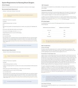
System Requirements:Windows *
Size:3.0 Gb
The software developer Altium is pleased to announce the availability of Altium Designer 22.9.1 Build 49, the PCB industry's leading design tool, allows engineers to focus more on designing and worry less about supply chain shortages.
Schematic Capture Improvements
Working in the Schematic with the 'Find Text - Jump' Dialog
The Find Text - Jump dialog is now a non-modal dialog, which means you can work with Altium Designer's interface including objects on the schematic sheet while the dialog is open.
This feature is in Open Beta and is available when the Schematic.FindTextAsModelessDialog option is enabled in the Advanced Settings dialog.
New Variant Manager
The process of managing variants in your design has been greatly enhanced. For creating, editing, and managing design variants, a new document-based Variant Manager is now available.
In addition to traditional variant management for specific components in the design, you now have the ability to create groups of components from a chosen schematic sheet, sheets referenced by a chosen sheet symbol, or a chosen component class with a functional-based view of component variations. For each group, you can define one or more 'options', which essentially reflect some variation of one or more components in the group. Variants themselves can then be created based on these defined groups and options, with support for creating a hierarchy of variants.
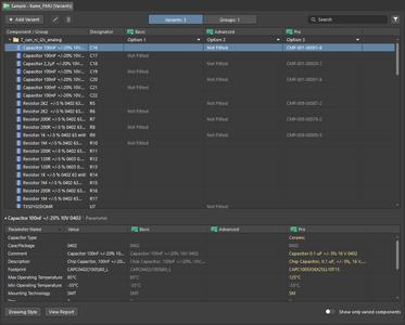
The new Variant Manager allows creating design variants based on options defined for component groups. Shown here is the Variants tab of the Variant Manager with three variants created and different options applied for a component group.
When a change is made, editing a value within a group option is instantly reflected in all variants that use that group option rather than having to change each varied component across each defined variant one at a time. The impressive time-saving efficiency gained in variant creation and editing will be appreciated by all users, especially those who deal with a sizable number of design variations. No matter if you are dealing with a handful of variants or hundreds, the new document-based variant management interface presents your variants in a far more readable form.
This feature is in Open Beta and is available when the Schematic.FindTextAsModelessDialog option is enabled in the Advanced Settings dialog.
PCB Design Improvements
Minimum Thermal Relief Conductor Gap for Custom Pad Shapes
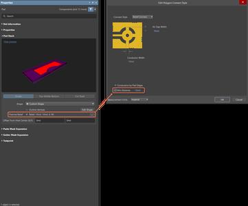
This release adds the ability to check the minimum gap between thermal relief conductors of custom pad shapes. The new Min Distance option is accessed by enabling the Thermal Relief option in the Pad Stack region of the Properties panel in Pad mode, then clicking the associated to the right of the option. The Edit Polygon Connect Style dialog opens. The new Min Distance option appears in the dialog when the Conductors by Pad Edges option is enabled. When Min Distance is enabled, you can enter the desired minimum distance of thermal relief conductors of the custom pad.
Added Detection of Zero Area Polygons in the Health Check Monitor
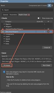
The Health Check tab in the Properties panel (accessed in Board mode) now gives you the ability to detect and delete polygons with zero areas. The new Zero Area Polygons field has been added to the Polygons category so now you are able to delete all of these polygons at once using the Fix Issues button in the Issues region.
Added Command to Place a Text Frame
To support the quick placement of a Text object in String and Frame modes implemented in a previous release, a new Text Frame command has been added to the main Place menu and the Active Bar of the PCB and PCB footprint editors in addition to the existing String command.
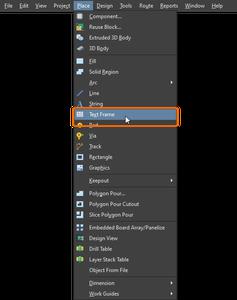

Use the new Text Frame command to quickly place a Text object in Frame mode.
When the Text Frame command is selected, Frame mode is active for the Text object being placed.
Improved Detection of Minimum Annular Ring Violation
Violations of the Minimum Annular Ring design rule can now be detected for pads and vias with connections on layers on which pad/via shapes are smaller than the pad/via hole (e.g., if pad/via shapes have been configured manually in the Properties panel or removed by using the Remove Unused Pad Shapes tool). An example of the new behavior is shown in the image below.
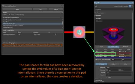
An example of the improved violation detection for the Minimum Annular Ring design rule.
Note that if a pad or via has its shape size less than the hole size but not equal to 0, this will also result in a violation of the Minimum Annular Ring design rule. Therefore, if a pad is used to define a mounting hole (without pad shapes), it is recommended to set its shape values to 0.
This feature is in Open Beta and is available when the PCB.Rules.MinimumAnnularRingConnected option is enabled in the Advanced Settings dialog.
Data Management Improvements
Alternative PCB Layouts in a Reuse Block
When creating a reuse block, multiple PCB models can now be added to it. To do this, use the Add New to Project » PCB command from the right-click menu of the reuse block's entry in the Projects panel.
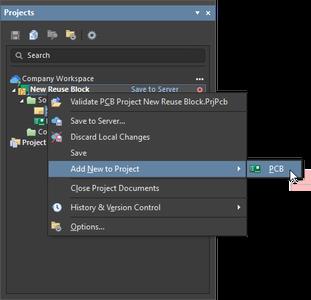
Use the Rename command from the right-click menu of the added PCB model's entry in the Projects panel to define a meaningful name for it. Use a Design » Update command from the schematic editor main menu to update the required PCB document.
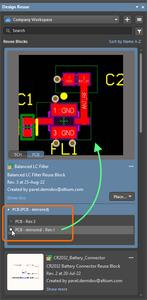
When the reuse block is saved to the Workspace, its PCB models are listed in the reuse block's PCB section within the Design Reuse panel that can be presented by clicking the Show more control within the reuse block's tile. Select the required PCB model in the list, and the reuse block will be placed with this model. The selected PCB model is shown in the preview area of the reuse block's tile when PCB is selected for preview.
Added 'Permissions' Property to Open Project Dialog
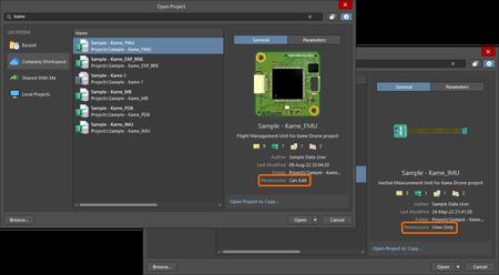
The new Permissions field that has been added to the Open Project dialog on the General tab for projects that are in a Workspace allows you to quickly see your permissions for the selected project: Can Edit or View Only.
Added 'View Only' Indicator in Projects Panel
Projects you have shared with viewing-only capabilities by using the Can View option in the Share dialog now display a new View Only indicator in the Projects panel. This non-clickable indicator is displayed for the user with whom you have shared the project.
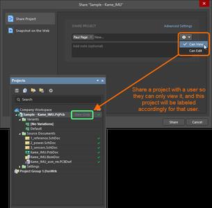
Note that a project shared with a viewer should be available for download for them so that they can open it in Altium Designer. Click the Advanced Settings control in the Share dialog to configure appropriate settings.
Improved Filter in the Comments and Tasks Panel
The filter in the Comments and Tasks panel (accessed by clicking the down arrow next to the filter icon) has been streamlined to eliminate any inaccuracies between the panel and the Tasks dashboard.
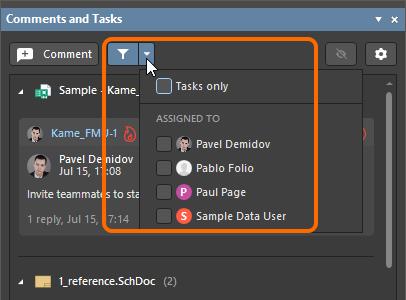
The filter has been updated to display the following:
- Tasks only - enable this option to show only comments that are assigned to a user.
- ASSIGNED TO - all options are disabled by default. Consequently, all tasks/comments are shown and sorted by name (the first entry in the list is the current user). When checkboxes are enabled, only the entries of those enabled will be displayed.
Note that the functionality for creating and managing tasks is not supported with the Altium Designer Standard Subscription. As such, with this level of access to Altium 365, this enhancement will not be available and the filter options in the Comments panel will be the same as in the previous release.
This enhancement is also not available when connecting to an Enterprise Server Workspace.
Ability to Add and Edit Comments in BOM Documents
This release added the ability to create and edit comments in an ActiveBOM document.
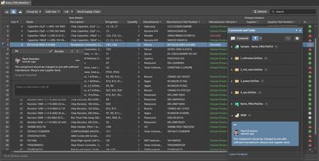
A comment can be added to a BOM item in the document in the following ways:
- Click the button available in the Comments and Tasks panel.
- Click near the top right-hand corner of the design space.
- Use the Tools » Comment command from the main menus.
After selecting a command, click on a row in the document to add a comment. Alternatively, right-click on a row then select the Comment command to add a comment to this row.
Enable Actionable VCS Status Icons
The feature that provides improved document VCS status has been enabled by default. To recap, this feature turns the VCS icons for project documents in the Projects panel into active controls that can be clicked to access more specific information, along with commands to perform applicable actions. This feature is accessed by the UI.ActionableDocumentStatuses option in the Advanced Settings dialog.
Circuit Simulation Improvement
Source of a Placed Component
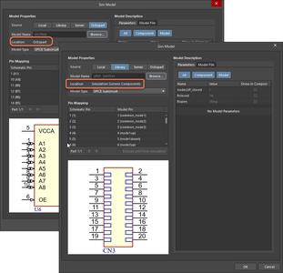
The sourced location of a placed component is now displayed in the Sim Model dialog in the Location field. This allows you to quickly see if the source used is the desired location.
Altium Designerrepresents decades of innovation and development focused on creating a truly unified design environment - One that enables users to effortlessly connect with every facet of the PCB design process. With features that have pioneered change and an ever-growing community of users, advocates, educators, and experts, Altium Designer is truly transforming the industry and pushing the boundaries of what's possible. Experience the world's finest PCB design product for yourself and see why more Engineers and Designers choose Altium than any other product available.
The Altium Designer 22 includes added features to help designers source component availability, enhanced capabilities that reduce manual design tasks, along with advanced real-time lifecycle management tools used in conjunction with Altium 365.
Altium Designer 22 Tutorial - Quick & Easy | Step by Step
After this tutorial you will know how to start designing your own boards in Altium Designer 2022 . For everyone who would like to learn Altium and also for everyone who has never ever designed any boards, but would like to learn how to do it. Enjoy!
Altium Ltd.is a multinational software corporation headquartered in San Diego, California, that focuses on electronics design systems for 3D PCB design and embedded system development. Altium products are found everywhere from world leading electronic design teams to the grassroots electronic design community. Founded in 1985, Altium has offices worldwide, with US locations in San Diego, Boston and New York City, European locations in Karlsruhe, Amersfoort, Kiev, Munich, Markelo and Zug, and Asia Pacific locations in Shanghai, Tokyo and Sydney.
Links are Interchangeable - No Password - Single Extraction


